Author:
Sara Rhodes
Date Of Creation:
11 February 2021
Update Date:
1 July 2024
Content
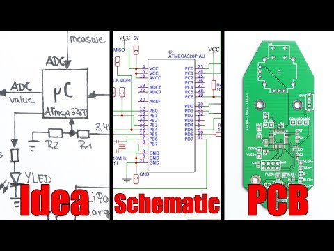
A homemade printed circuit board (PCB) is often used in robotics and electronics. Here are the basic steps for creating a PCB.
Steps
 1 Creating your board. Use PCB computer-aided design (CAD) software to create your PCB. You can also use a perforated board with pre-drilled holes in it to help you see the placement of components on the board layout and how it will look in reality.
  2 Purchase foil-clad textolite from a retailer, covered with a thin layer of copper on one side.
 3 Rub the PCB with an emery sponge and water to clean the copper backing from dirt. Dry the future board.
  4 Print your board schematic onto the matte side of a sheet of blue carbon paper. Make sure the direction of your drawing is oriented correctly to transfer it to the board correctly.
 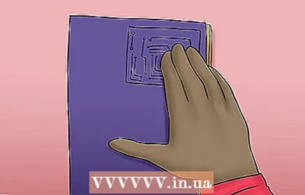 5 Place the blue tracing paper with the circuit printed on it on the copper side of the board.
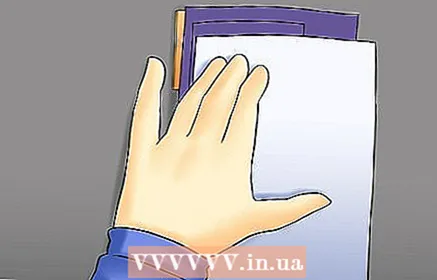 6 Place a sheet of plain white paper on top of blue carbon paper. Following the transfer instructions for the copy paper, iron the white paper to transfer the circuit from the copy paper to the copper surface of the board. Iron each part of the pattern well with the tip of the iron from the edges of the board.
  7 Let the board and blue paper cool. Carefully remove the blue paper from the board and look at the transferred drawing.
  8 Examine the copy paper for black print toner that could not be transferred to the copper backing. Make sure the pattern on the board is oriented correctly.
  9 Fill in the toner gaps on the board with black permanent marker ink. Let the ink dry for a few hours.
 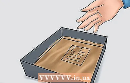 10 Remove exposed copper from the board with iron chloride using a process called etching.
- Put on your old clothing, gloves and safety glasses.
- Dip warm ferric chloride, stored in a rustproof container with a lockable rustproof lid, in a bucket of warm water. Do not heat it above 46 C to prevent the release of toxic fumes.
- Pour enough ferric chloride into a plastic tray with plastic holders to support the circuit board. Perform this operation in a well-ventilated area.
- Use plastic tongs to position the card face down in the tray on the holders. Keep it there for 5 to 20 minutes, depending on the size of the board, to dissolve the unwanted portions of the copper. Use plastic pliers to rinse the board in the tray of solution to speed up the etching process, if necessary.
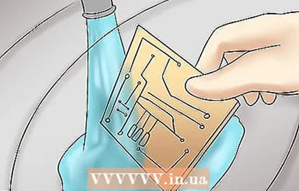 11 Thoroughly wash all etch fixtures and the circuit board in plenty of running water.
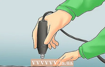 12 Use a 0.8mm HSS or carbon steel drill to drill holes for your board components. Wear safety goggles and a face shield to protect your eyes and lungs while drilling.
  13 Wipe the board with a clean sponge and water. Replace the electrical components and solder them.
Tips
- Always use old clothing, goggles, and gloves when working with ferric chloride or other chemically hazardous substances during pickling.
- Read a book on How to DIY a PCB to help you understand the design and construction process.
- Ammonium persulfate is an alternative chemical reagent to iron chloride for etching the board.
Warnings
- Pickling chemicals can stain clothing or plumbing fixtures. Store all herbal chemicals safely and use caution when using them.
- Never pour used ferric chloride through metal pipes or store it in a metal container. Iron chloride is very toxic and corrodes metal.
What do you need
- Computer
- Printer
- CAD programs
- Printed drawing
- PCB board covered with copper foil
- Emery sponge
- Water
- Blue carbon paper
- White paper
- Iron
- Black permanent marker
- Old clothes
- Safety glasses
- Gloves
- Herb material
- Drill with bits
- Protective mask
- PCB components
- Tinning tool


